Read this
first:
Copyright
(c) 2008 Nard Awater
All
rights reserved.
Redistribution
and use in source and binary forms, with or without
modification, are permitted provided that the following conditions
are met:
1.
Redistributions of source code must retain the above
copyright notice, this list of conditions and the following
disclaimer.
2.
Redistributions in binary form must reproduce the above
copyright notice, this list of conditions and the following
disclaimer in the documentation and/or other materials
provided with the distribution.
3.
Neither the name of the author nor the names of the
contributors may be used to endorse or promote products
derived from this software without specific prior written
permission.
THIS
SOFTWARE IS PROVIDED BY THE AUTHORS AND CONTRIBUTORS ``AS IS'' AND
ANY EXPRESS OR IMPLIED WARRANTIES, INCLUDING, BUT NOT LIMITED TO, THE
IMPLIED WARRANTIES OF MERCHANTABILITY AND FITNESS FOR A PARTICULAR
PURPOSE
ARE DISCLAIMED. IN NO EVENT SHALL THE AUTHORS OR CONTRIBUTORS
BE LIABLE
FOR ANY DIRECT, INDIRECT, INCIDENTAL, SPECIAL, EXEMPLARY, OR
CONSEQUENTIAL
DAMAGES (INCLUDING, BUT NOT LIMITED TO, PROCUREMENT OF SUBSTITUTE GOODS
OR SERVICES; LOSS OF USE, DATA, OR PROFITS; OR BUSINESS INTERRUPTION)
HOWEVER CAUSED AND ON ANY THEORY OF LIABILITY, WHETHER IN CONTRACT,
STRICT
LIABILITY, OR TORT (INCLUDING NEGLIGENCE OR OTHERWISE) ARISING IN ANY
WAY
OUT OF THE USE OF THIS SOFTWARE, EVEN IF ADVISED OF THE POSSIBILITY OF
SUCH DAMAGE.
Tools page
Schematic entry
In the technical part of
this website, http://www.aplomb.nl/TechStuff/TechStuff.html
, you may find schematics that are usefull to you. In general, I put a
.png-file in that you can right-click to download or left-click to
view. But if you wish to adapt the design, re-doing all CAD-work is a
waste of time. Therefor I also provide a .sch-file
in. To edit these files, you need a program: ExpressSchematic. It's
part of the design-chain as supplied by ExpressPCB. They produce (you
guessed that of course): Printed Circuit Boards. Have a look at their
site and services: http://www.expresspcb.com/ And since you're there: download
the program as well.
I chose this program as it's far more intuitive (to me) than the more
commonly used Eagle-program.
For ExpressSch I created lots of schematic symbols, intended for personal use. But I don't mind sharing it.
Legal note: the presented information is not guaranteed to be correct. Use at your own risk. Like I do ....
Here it is: ExpressSch symbols Plons dec2008
I did not create the pcb-symbols for these symbols .... it's just for schematic entry.
If you want to share your work as well, contact me at : and now there
should be an email address. Unfortunately we live in a world where
Spammers abuse this information. Therefor: contact me at http://www.avrfreaks.net
. My username there is Plons. Send me a PM, and I will send you an
email address. Sorry for this inconvenience, but that's how it is ....
As an alternative: send a mail to "tools", without quotes, then
the curly symbol you find in every email-address, and then the domain:
you can find it in the address-bar of your browser.
PCB design
So far I didn't provide a lot of layouts for PCB's, but that may
change: if a design is available, you can view it with this ViewLayout50_eng
(right-click to download)
It allows you to print my PCB-designs on your own printer on the
material you choose. It also has some tools for calibrating the
printer. Check the artwork before actually making a PCB.
Note: there were problems reported with the ViewLayout50-file, so I
replaced it with a compressed version. Most likely we are "protected"
from contents that possibly could damage our PC ..... sigh.
And here is the German version: viewlayout50_german
Download
ViewLayout50 and put it on
your desktop (no need for an
install), unzip it to your desktop, it's just 1 executable file. Then download the layout, put it on your desktop as well,
start ViewLayout50, do File --> Open, select <filename>.lay.
The
viewer doesn't allow you to change the file, just to view or print it.
It's all in the name huh ;-)
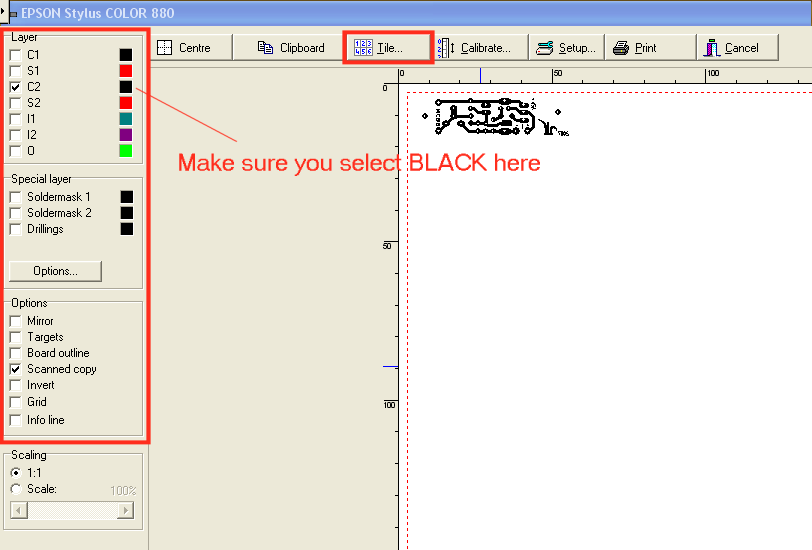
Next, do File --> Print, and set the screen as the capture shows
here. If you want to make more boards , use Tile. The program also
allows you to calibrate your printer. Just take some time to explore
all possibilities. In order for you to calibrate, there are two layouts that can be used for that: Cal grid mm.lay and Cal grid inch.lay
Check the "Scanned Copy" if you want to see my Aplomb-logo on the PCB.
And choose black as color. Note: not all PCB's will use that.
Make sure to UNTICK all layers except C2 when printing; and choose black as color for C2 !!
So far, all designs are single sided. I "abuse" the top-layer to make
wire connections. And sometimes even the silk-screen is used for that.
Layer C2 is the copper-layout, the rest is bonus, and usefull for a
paper-plot. You will have to sort out yourself where which components
should be placed; like said, there is no link between schematic and
layout. So it's a bit of a puzzle. But once you start, you'll find it's
not that hard.
For SprintLayout I created lots of symbols, intended for personal use. But once more, I don't mind sharing it :)
Legal note: the presented information is not guaranteed to be correct. Use at your own risk. Like I do ....
Here it is: SprintLayout_symbols_Nard_jan_2009
Enjoy !!
Plons, December 2008
fe